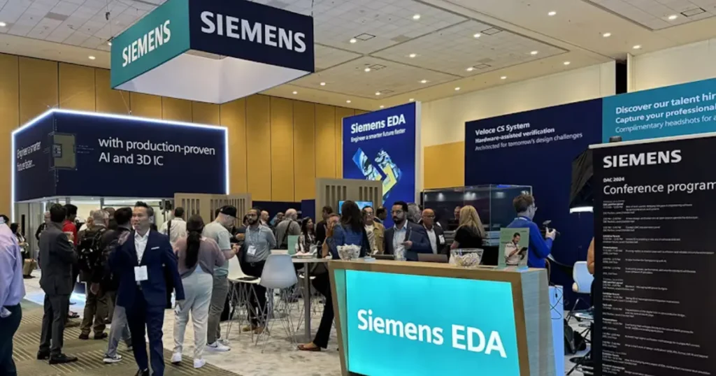
At DAC 2025, Siemens Digital Industries Software unveiled two new tools designed to enhance the manageability, predictability and success of 3D IC design.
As 2.5D and 3D Integrated Circuits (IC) become increasingly vital in advanced chip design, traditional EDA workflows are under pressure. Rising complexity, thermal management issues and integration risks are pushing design teams to seek advanced design and test solutions.
At this year’s Design Automation Conference (DAC), Siemens announced the expansion of its EDA portfolio with two targeted solutions: Innovator 3D IC™ and Calibre 3DStress. Together, these tools are designed to reduce design risk. Enhance reliability and help engineering teams improve the predictability and quality of next-generation IC delivery.
Tackling the Realities of 3D IC Design
3D IC, or three-dimensional integrated circuit design, refers to the vertical stacking and interconnection of multiple die onto a single package. It’s a powerful way to increase functionality, performance and density but it also introduces a new level of design complexity that needs to be addressed.
As devices shrink and system-in-package (SiP) designs become all the more common, the need for simulation and analysis tools that can handle this complexity has become top of the list for chip architects, layout engineers and verification teams alike – especially those navigating the challenges of next-generation 2.5D and 3D integration.
What Siemens Announced at DAC 2025
1. Innovator 3D IC™ Solution Suite
The new Innovator 3D IC suite functions as a full-stack integration environment purpose-built for planning, simulation and data management in 2.5D and 3D IC architectures.
Built with AI-enhanced usability, multithreading and multicore performance, the platform is optimized to handle designs with over 5 million pins.
The suite includes four tightly integrated components:
- Innovator3D IC Integrator: A centralized cockpit for building a digital twin of the 3D IC system
- Innovator3D IC Layout: A correct-by-construction package for interposer and substrate implementation
- Innovator3D IC Protocol Analyzer: Focused on interface compliance, this tool checks chiplet-to-chiplet and die-to-die protocols
- Innovator3D IC Data Management: Handles work-in-progress and version control of complex design data and IP
This modular architecture gives chip design teams the flexibility to simulate and implement heterogeneous multi-die systems, aiming to reduce integration friction while improving project predictability.
2. Calibre 3DStress
As designs move into thinner dies and experience higher thermal loads during packaging, traditional die-level validation is no longer sufficient. What works initially can be compromised after reflow, as heat and mechanical pressure change the shape of the chip and affect how it works electrically.
Calibre 3DStress is designed to address this challenge by enabling early, transistor-level simulation, verification and debugging of thermo-mechanical stress and warpage within the context of 2.5D and 3D IC packaging. By modeling real-world chip-package interactions before tape-out, teams can detect design weaknesses that may otherwise lead to costly silicon failures.
Part of Siemens’ growing multiphysics portfolio, Calibre 3DStress builds on the foundation of Calibre 3DThermal, integrating a native mechanical solver with Siemens’ industry-standard verification engine. This supports engineers to:
- Predict how stress affects transistor performance
- Evaluate material deformation and interconnect strain
- Optimize layouts for durability, reliability and yield
Calibre 3DStress is designed to provide deep visibility and deliver engineers actionable insights during critical stages of the design process.
Why This Matters for ASIC Development Teams
For engineers working on advanced nodes, the stakes are high. A single thermal mismatch or integration error can result in substantial NRE costs, significant schedule setbacks and project reliability issues. By addressing these concerns head-on with purpose-built EDA tools, Siemens is equipping chip design teams with actionable insight at critical points in the development cycle.
From architecture to analysis, and simulation to sign-off, Siemens, by unveiling these new tools, aims to frame 3D IC complexity as a challenge that can be effectively addressed.
Advancing 3D IC Design
As the semiconductor industry embraces 2.5d and 3D packaging as a path forward, the tools to support that vision must evolve. Siemens’ announcement at DAC 2025 represents a step in the right direction – bringing integrated, stress-aware design into sharper focus.
Alongside Siemens, other leading EDA vendors such as Synopsys and Cadence continue to invest heavily in 3D IC and advanced packaging solutions, developing platforms that address the growing complexity of chip design and verification in 2025.
For teams tackling high-stakes integration and next-generation architectures, this could contribute to achieving more robust, reliable and repeatable silicon results.