ASICs and FPGAs are both essential parts of modern hardware design – but it’s important to understand that they solve different problems at different points in the silicon lifecycle. Whether you’re prototyping new IP or delivering final production, choosing between them involves more than just cost or performance – flexibility, timelines and verification strategy all play critical roles.
This introductory guide breaks down what sets ASICs and FPGAs apart, offering a clear comparison of design tradeoffs, real-world use cases and insights into how each fits within today’s verification workflows. From early prototyping to production-grade tapeouts, here’s what every engineer needs to know when navigating the FPGA-to-ASIC journey.
What is an ASIC?
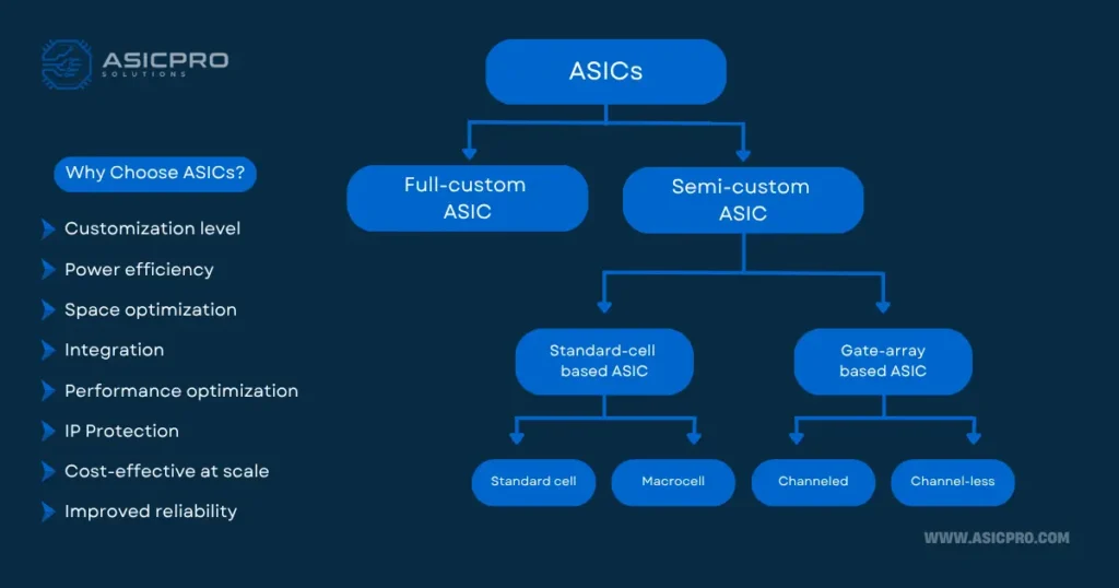
An application-specific integrated circuit (ASIC) is a custom-designed chip optimized for a specific task. Once manufactured, an ASIC’s function is fixed – making them ideal for high-volume, high-performance applications such as smartphone SoCs, automotive ADAS systems and AI inference accelerators.
However, ASIC development requires significant investment in time and resources, including high non-recurring engineering (NRE) costs and multi-stage verification.
Verification for ASICs involves extensive simulation, emulation, formal analysis and regression testing – all completed before tapeout to minimize the risk of costly silicon respins.
What is an FPGA?
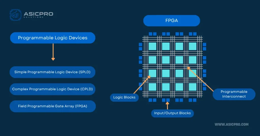
A field-programmable gate array (FPGA) is a a reconfigurable logic device that allows engineers to implement and test digital circuits without fabricating new silicon. Composed of configurable logic blocks and programmable interconnects, FPGAs enable rapid iteration during early design and testing phases.
Common FPGA uses include:
- Early-stage prototyping
- Algorithm validation
- Post-deployment updates in systems where reconfigurability is key
FPGAs are especially useful in hardware-assisted verification, where they serve roles in emulation, FPGA-in-the-loop (FIL) and hardware-in-the-loop (HIL) test environments. While FPGAs offer flexibility and fast turnaround, they generally have lower performance, higher power consumption and higher per-unit costs compared to ASICs.
ASIC vs FPGA: A Side-by-Side Comparison
| Feature | ASIC | FPGA |
|---|---|---|
| Design Purpose | Fixed function, custom silicon | Reprogrammable logic |
| Performance | Very high (optimized at design level) | Moderate |
| Power Efficiency | Excellent | Lower (programmable fabric overhead) |
| Time to Market | Longer (fab & NRE cycles) | Shorter (no fabrication required) |
| Unit Cost (at Volume) | Low | High |
| NRE Cost | High (custom masks, layout, etc) | Low (no custom silicon – standard off-the-shelf parts) |
| Flexibility | None post-fabrication | High (reconfigurable at any time) |
| Use Cases | SoCs, AI chips, automotive, IoT | Prototyping, aerospace, industrial, defense |
| Verification Tools | UVM, formal, emulation, full regression | Prototyping, FPGA-in-loop, HIL |
Where do ASICs and FPGAs Excel?
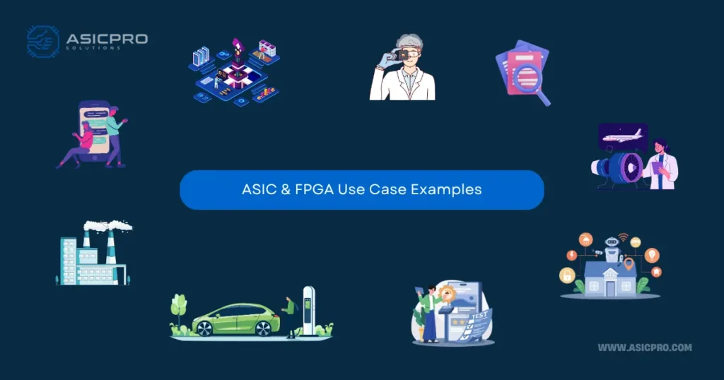
Understanding how ASICs and FPGAs are used in real-world systems helps clarify where each shines. These examples show the practical use of both technologies across various domains:
ASIC Use Cases:
- Smartphones and SoCs: Custom ASICs drive high performance and low power in mobile processors and RF components
- AI and Data Centre Acceleration: ASICs like TPUs or custom inference engines are optimized for speed and throughput
- Automotive Safety Systems: Functional safety, reliability and real-time performance make ASICs the go-to for ADAS and braking systems
- Consumer IoT Devices: ASICs minimize power draw and cost in wearables, sensors and smart home products
FPGA Use Cases:
- Aerospace and Defense: Reprogrammability allows updates after deployment and secure on-site logic changes
- Pre-Silicon Prototyping: FPGAs play a central role in validating ASIC IPs before tapeout through emulation and hardware-in-the-loop (HIL) testing
- Industrial Control Systems: Flexibility and field updates make FPGAs suitable for evolving automation tasks
- Academic and R&D: Ideal for testing novel architectures and experimental algorithms with no fabrication required
The FPGA-ASIC Journey
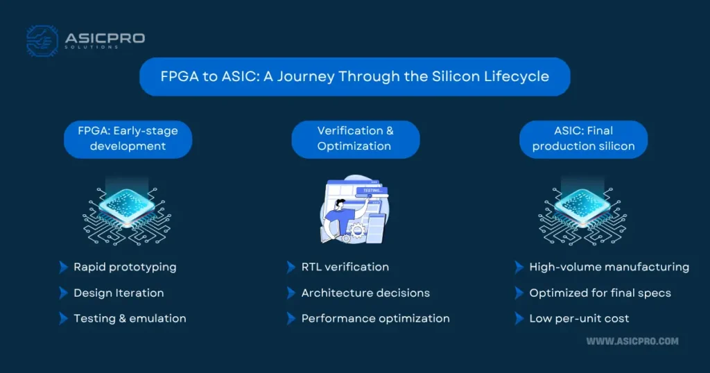
- FPGAs shine during early development, IP validation and use cases requiring adaptability
- ASICs dominate where efficiency, performance and scalability matter most – especially in final production environments
- Verification is key across both, but the stakes increase dramatically when moving from FPGA prototypes to final ASIC tapeout
Success depends on early investment in architecture planning, testbench development and verification toolchains that scale from pre-silicon stages to final production.
What’s Next?
In upcoming articles, we’ll dive deeper into:
- Behind the Chip: Exploring Real-World ASIC Applications
- Hardware-Assisted Verification: A Smarter Way to Accelerate Chip Development
- What is a System on Chio (SoC)? A Practical Guide for ASIC Engineers
- The ASIC Verification Landscape in 2025: Trends, Tools and More
Stay tuned and follow us on LinkedIn for the latest news from across the world of semiconductors.