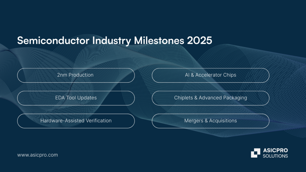
Semiconductor Industry Milestones 2025
As 2025 comes to a close, it’s an ideal time to reflect on the trends and developments that shaped the semiconductor industry this year. From advances in process technology to the rise of chiplet architectures and AI-optimised silicon, 2025 has been a year or progress and innovation for chip design teams and verification engineers. In this article, we highlight the milestones that defined the year and their implications for ASIC designers and verification specialists.
2nm Production Edges Closer to Mainstream
Leading foundries made significant strides towards 2nm chips, improving transistor density while keeping power consumption under control. These advances are critical for meeting the growing demands of high-performance computing and AI workloads. From Marvell and TSMC demonstrating AI-optimised 2nm silicon to other industry leaders pushing early adoption in niche ASICs, 2025 further set the stage for next-generation compute performance, enabling designers and verification teams to explore higher-speed, lower-power architectures than ever before.
AI & Accelerator Chips
The demand for on-chip AI acceleration continues to drive investment in custom architectures, powering everything from cloud AI inference to edge devices. Companies focused on integrating AI cores and tensor engines into ASICs, allowing for greater performance-per-watt while introducing new verification challenges. Hardware-assisted verification and early formal methods increasingly became essential to validate complex designs, helping engineers identify corner-case issues before silicon fabrication.
EDA, AI Innovation & Design Methodology Shifts
EDA tools continued their rapid evolution in 2025, with AI increasingly embedded to optimise placement, routing and timing closure. Siemens launched Questa One to simplify chip verification, while Synopsys introduced ZeBu-200 and HAPS-200 hardware-assisted verification platforms to accelerate complex RTL testing. Accellera also approved the UVM-MS 1.0 standard for mixed-signal verification, providing engineers with a more structured methodology for modern multi-domain designs. Together, these advances are reshaping how designers and verification teams approach ASIC development, enabling faster iterations without compromising coverage or reliability.
Chiplets & Advanced Packaging
Chiplet architectures gained significant traction both in industry conversation and real-world applications as a scalable approach to increase performance while controlling cost and yield. Companies demonstrated multi-die integrations and modular designs that allow engineers to tackle system-level challenges with greater flexibility. For verification teams, these architectures continue to introduce new testing requirements, particularly around cross-chiplet connectivity, corner-case scenarios and integration timing. As of 2025, chiplets can no longer be classed as experimental – they are fast becoming a practical approach for many high-performance designs.
Strategic Partnership & Ecosystem Growth
Collaborations between industry leaders accelerated innovation in both design and verification. Cadence’s acquisition of ChipStack strengthened AI-powered verification capabilities, while Qualcomm’s acquisition of Arduino enhanced edge AI and embedded prototyping. NVIDIA partnered with Synopsys to optimise AI-driven design workflows, and Synopsys completed its acquisition of Ansys, expanding the ecosystem of verification tools. These strategic moves underscore the growing importance of collaboration and early engagement with partners, particularly when integrating IP blocks into complex ASICs.
The Rise of Hardware-Assisted Verification & Smart Solutions
Verification teams increasingly pushed formal and hardware-assisted verification earlier in the design flow, catching corner-case bugs sooner and improving overall confidence in designs. Tools like Synopsys’ ZeBu-200 and HAPS-200, alongside Siemens’ Questa One platform, allowed teams to validate more complex designs faster than ever before. As verification workloads become more complex, hardware-assisted solutions are no longer optional – they are a critical component of efficient, high-coverage ASIC verification.
Rapid Expansion of National Chip Strategies
Countries across the globe continue to invest heavily in domestic semiconductor capabilities, boosting local expertise, IP development, and advanced packaging initiatives. For engineers and design teams, these national strategies influence supply chains, IP availability, and verification approaches, requiring careful planning and collaboration across ecosystems.
Looking Ahead: Lessons and Opportunities for ASIC Designers and Verification Teams

As we come to the end of another busy year, the semiconductor stands industry at a monumentous junction. The advances we’ve seen this year – from 2nm process technology and AI-optimized silicon to the adoption of chiplets and hardware-assisted verification – are more than incremental improvements; they represent an important shift in how engineers design, validate, and bring silicon to market.
For ASIC designers, these trends highlight the growing importance of modular, high-performance architectures that can meet the diverse demands of AI, edge computing and more. Verification specialists, in turn, must adapt to increasingly complex workflows, leveraging hardware-assisted solutions, early formal verification and AI-driven EDA tools to ensure coverage and reliability. Supply chains, IP integration and cross-collaboration between partners now play a critical role in successful chip development.
Looking ahead, 2026 promises to build on these trends. AI-accelerated design flows will become even more mainstream, chiplet architectures will expand into new markets and verification teams will continue to adopt smarter, earlier and more automated approaches.
For engineers and teams who stay informed and proactive, the opportunities to innovate, optimise and influence the next generation of semiconductors are immense.