
Semiconductor News & Industry Developments

December closed out 2025 with a strong mix of design breakthroughs and strategic partnerships across the semiconductor ecosystem. From hyperscaler AI infrastructure and advanced memory research to new design hubs and talent initiatives, this month’s roundup highlights the developments shaping how chips are designed, verified, and manufactured.
Below, you’ll find the key news stories, followed by notable technical reads and industry updates worth bookmarking.
NVIDIA & Synopsys Expand Strategic Partnership
NVIDIA and Synopsys announced an expanded collaboration aimed at transforming engineering and design workflows for AI-driven systems. The partnership brings together NVIDIA’s accelerated computing platforms with Synopsys’ EDA and simulation technologies to support increasingly complex AI, HPC and system-level designs. The move reflects the growing convergence of silicon, software and AI-powered engineering.
Samsung Researchers Explore Low-Power NAND Design
Samsung researchers published a novel NAND memory design based on ferroelectric transistors, reporting up to 96% lower power consumption compared to conventional approaches. While still in the research phase, the work highlights how materials innovation could significantly impact energy efficiency for future storage and memory-intensive AI workloads.
Openchip Launches New Design Centre in Ireland
Openchip is expanding its European presence with a new design centre in Ireland. The facility will support advanced SoC development for high-performance computing and AI, further strengthening Ireland’s position as a growing hub for semiconductor design and engineering talent.
Siemens and Certus Semiconductor Partner for AI-Driven Analog Design
Siemens Digital Industries Software and Certus Semiconductor announced a partnership focused on applying AI to analog, IO and ESD design. By combining Siemens’ EDA tools with Certus’ analog IP expertise, the collaboration aims to improve design productivity, robustness and scalability for increasingly complex mixed-signal systems.
ARM Announces Plans for Semiconductor Design School in South Korea
Arm shared plans to establish a semiconductor design school in South Korea, with a goal of training more than 1,400 chip design professionals. The initiative underscores a growing industry consensus: talent development is now as critical as process technology in sustaining long-term semiconductor innovation.
HCLTech and Dolphin Semiconductor Announce Plan to Co-develop energy-efficient chips
HCLTech and Dolphin Semiconductor announced plans to jointly develop low-power chips targeting IoT, automotive, and data-centric applications. The collaboration focuses on energy efficiency and mixed-signal expertise, aligning with broader industry demand for power-optimised edge and embedded silicon.
Siemens & Toshiba Collaborate on EDA and System Design
Siemens and Toshiba have partnered to advance electronic design automation (EDA) and system-level integration workflows. The collaboration aims to improve productivity and accuracy in complex SoC and semiconductor projects, reflecting a growing trend of cross-company cooperation to accelerate design innovation.
S2C, MachineWare and Andes Introduce RISC-V Co-Emulation Solution
S2C, MachineWare, and Andes have jointly launched a RISC-V co-emulation platform designed to accelerate chip development. The solution enables hardware/software teams to test designs earlier, reduce risk, and shorten development cycles for RISC-V-based SoCs.
Siemens and nVent Collaborate on Liquid Cooling and Power Architecture
Siemens and nVent announced a partnership focused on liquid cooling and power distribution solutions for high-performance computing and semiconductor manufacturing. Their collaboration seeks to optimise thermal management and energy efficiency, supporting more reliable, high-density computing infrastructure.
Technical Reads & Research Highlights

| Title | Source |
|---|---|
| Autonomous ASIC Root Cause Analysis | SemiEngineering |
| The Evolution of Embedded Computing Beyond Moore’s Law | Embedded |
| How AI and Virtual Twins Can Supercharge Semiconductor Yield | EE Times |
| AI In A/MS IC Design: Between Buzzword And Productivity Boost | SemiEngineering |
| Addressing the Biggest Bottleneck in the AI Semiconductor Ecosystem | EE Times |
| Chiplet Technology in Automotive Applications: A Cost-Effective Path to Advanced Electronics | Embedded |
| Design specification: The cornerstone of an ASIC collaboration | EDN |
| Software-Defined Hardware-Assisted Verification: Scaling To Quadrillions Of Cycles For Verification In The AI Era | SemiEngineering |
| The Rise Of The TPU: Innovating For Specialization | Forbes |
| Generative AI: The Booster for the Software-Defined Vehicle | Design News |
| Formal Verification Techniques and Reliability Methods for RRAM-based Computing-in-Memory | SemiEngineering |
| LLM-based Behaviour Driven Development for Hardware Design | SemiEngineering |
Videos
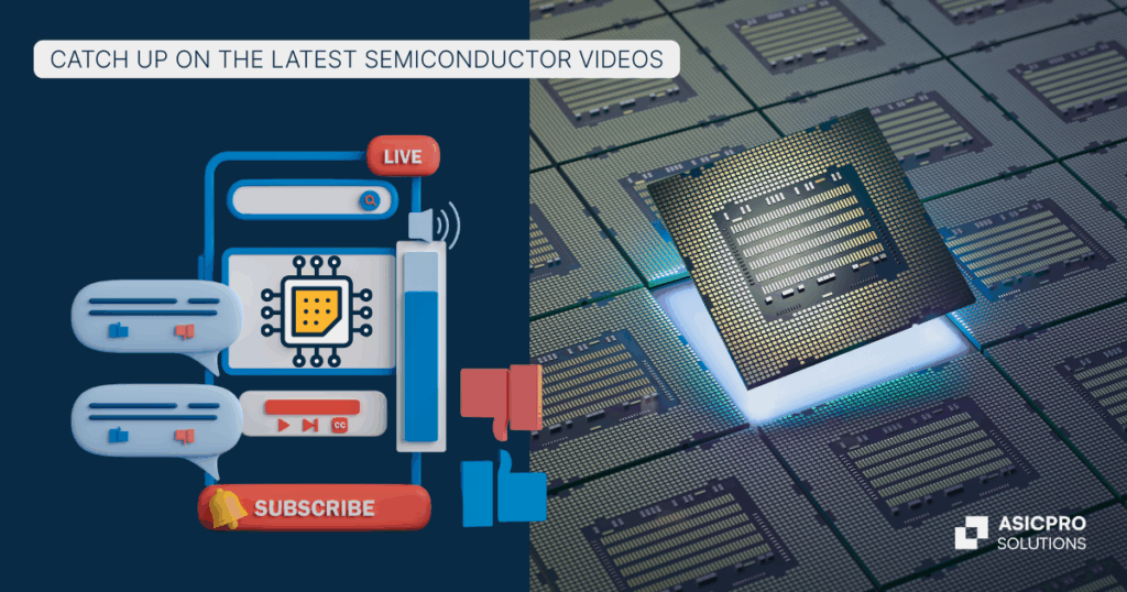
Explore the latest videos exploring chiplets, verification and multi-die design:
- DFT Shifts Further Left: Jeff Meyer (Siemens EDA) discusses evolving DFT strategies for multi-die assemblies.
- The State of Multi-Die: The EE Times Tech Podcast explores customer requirements and design challenges in advanced packaging.
Your Monthly Roundup: What’s Next for Semiconductors?
December 2025 highlighted continued momentum across AI infrastructure, chiplet-based design, verification workflows and power-efficient architectures. As complexity grows across systems, silicon and software, collaboration, automation and talent development are becoming just as critical as process scaling.
Stay tuned for future editions as we continue tracking the technologies and trends shaping the next generation of chips.
Interested in contributing to these developments? Visit our careers page to explore opportunities in ASIC design, verification and semiconductor engineering.