Electronic Design Automation: A Practical Guide for Engineers
As semiconductor complexity continues to surge, Electronic Design Automation (EDA) tools have become the backbone of modern chip development. These vital software platforms enable engineering teams to design, verify, implement and validate semiconductor devices with the speed, accuracy and confidence required in today’s competitive landscape.
Ultimately, EDA tools are the engines that make ASIC design possible at scale. Without them, today’s highly-integrated SoCs – often containing tens of billions of transistors – couldn’t exist.
As defined by Synopsys, EDA encompasses the software, hardware and services that support the definition, planning, design, implementation, verification and manufacturing of semiconductor devices.
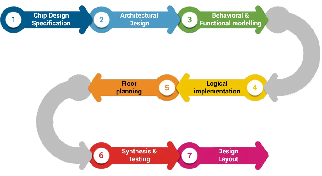
What is EDA and Where Does It Fit in the ASIC Flow?
EDA underpins every stage of chip creation, from early architectural exploration to RTL development, simulation, physical implementation and hardware-assisted verification.
Engineers rely on EDA tools to:
- Write and optimise RTL
- Validate functionality and coverage
- Perform structural checks (CDC, linting, DFT)
- Implement physical layout and optimise PPA
- Run timing, IR-drop and power sign-off
- Emulate and prototype complex SoCs before tape-out
Why EDA Matters
Chip teams today face unrelenting demands: shrinking timelines, massive compute workloads, increasingly advanced nodes and new security expectations. EDA directly addresses these pressures by enabling:
- Faster design and verification cycles
- Higher functional and structural confidence
- Better PPA closure at advanced nodes
- Reduced respin risk through earlier bug discovery
- Scalability compute for AI/ML-assisted tasks
With AI hardware startups and hyperscalers compressing multi-year development cycles into months, EDA tools – especially when paired with cloud workflows and hardware-assisted verification – remain essential to keeping pace with innovation.
Key EDA Tools by Design Stage
These leading platforms streamline the path from RTL to tape-out, ensuring designs meet timing, power, reliability and manufacturability requirements.
| STAGE | Purpose | Key EDA Tools |
|---|---|---|
| Front-End (Design & Verification) | RTL design, linting, simulation, formal verification | Synopsys Design Compiler, Cadence Genus, Synopsys VCS, Cadence Xcelium, Siemens Questa, SpyGlass, JasperGold |
| Physical Implementation | Place & route, timing closure, power optimization, layout sign-off | Synopsys IC Compiler II, Cadence Innovus, PrimeTime, Tempus, Voltus |
| Acceleration & Prototyping | Hardware-assisted verification & system-level testing | Synopsys ZeBu, Cadence Palladium, Siemens Veloce |
Trends Shaping the Future of EDA
The EDA ecosystem continues to evolve rapidly to ensure its aligned to industry trends and demands:
- AI-Driven Automation: ML-powered optimisation and generative design flows are reducing manual effort and enabling predictive closure
- Cloud-Native EDA: Cloud-based simulation, sign-off and emulation make it possible to scale compute resources dynamically – this is critical for AI accelerators and large SoCs
- Security-Driven Design: Earlier insertion of hardware security mechanisms and ISO 26262 compliance for automotive and edge AI
- The “Silicon-to-Systems” Approach: EDA is expanding beyond chip design into system-level modelling, software co-development and lifecycle support – aligning more closely with product-level requirement
Industry Outlook
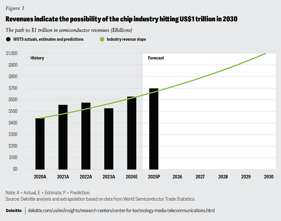
Deloitte’s 2025 Global Semiconductor Industry Outlook predicts the market will reach $697B by the end of 2025, driven heavily by the demand for generative AI silicon. Longer term projections suggest semiconductor revenue could reach $2T by 2030.
However, achieving this growth depends on overcoming several challenges:
- Escalating design complexity at advanced nodes
- Talent shortages across all aspects of ASIC development
- Growing security and compliance requirements
- The need for seamless hardware/software co-design
As these pressures intensify, EDA vendors are accelerating their own internal innovation cycles. The shift towards AI-driven automation and cloud-native workflows signals a broader transformation. EDA is moving from being a toolset to a strategic enabler – reshaping the engineering process itself and empowering teams to deliver higher-quality silicon faster.
Signing-off
EDA is no longer just a means to complete chip design. It is a competitive differentiator for companies building advanced SoCs, AI accelerators and complex, interconnected systems.
If you’re exploring how to optimise your EDA flow, accelerate verification or scale your next ASIC project, our engineering team can help. Reach out – we’d love to discuss how we can best support your roadmap.